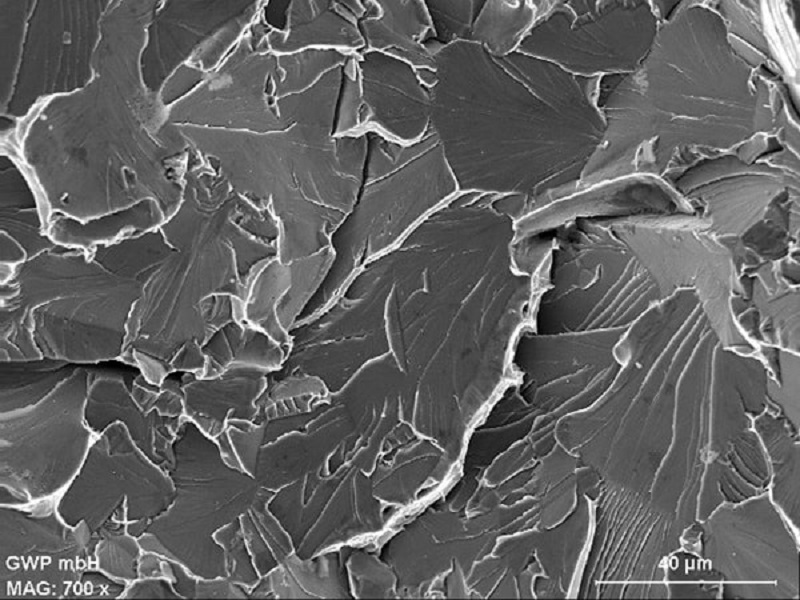
Scanning electron microscopy SEM
In the scanning electron microscope, the surface of the sample is displayed with a high depth of field. A tungsten cathode is used to generate an electron beam that scans the surface of a sample in a high vacuum. The resulting interaction products are detected and provide image information about the surface properties. By means of secondary or backscattered electron contrast, various forms of representation can be selected. This makes it possible to evaluate fracture surfaces or topographies of plastic components in great detail.
To be able to resolve an image in the SEM, the sample must be conductive. In the case of plastic samples, this is done by vapour deposition with an extremely fine gold or graphite layer. In addition, it is possible to handle the sample in a low vacuum.
The GWP plastics laboratory operates two scanning electron microscopes with the following applications:
Imaging by secondary or backscattered electron contrast
Resolution in the 2-digit nm range (50,000-fold)
Operation with low vacuum (1 to 270 Pa) possible (no vapour deposition of the sample necessary)
EDX elemental analysis with silicon drift detector
Large sample chamber: samples with diameters up to 200 mm, 70 mm height and up to 2 kg weight.
SEM examinations are used for the analysis of structural anomalies and damaged areas in surfaces as well as for structural examinations in polymer blends or composite materials.


